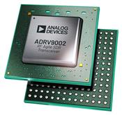
ADRV9002BBCZ
Stock Availability: 0
| Manufacturer: | Analog Devices, Inc. (ADI) |
|---|---|
| Mfg #: | ADRV9002BBCZ |
| Richardson RFPD #: | ADRV9002BBCZ |
| Description: | Multi-Function Transceiver |
| Min/Mult: | 1 |
| Datasheet |
ADRV9002BBCZ |
| EDA/CAD Models |
|
The ADRV9002 is a highly integrated, RF transceiver that has dual-channel transmitters, dual-channel receivers, integrated synthesizers, and digital signal processing functions.
The IC delivers a versatile combination of high performance and low power consumption required by battery powered radio equipment and can operate in both FDD and TDD modes. The ADRV9002 operates from 30 MHz to 6000 MHz and covers the UHF, VHF, licensed and unlicensed cellular bands, and industrial, scientific, and medical (ISM) bands. The IC can support both narrowband and wideband standards up to 40 MHz bandwidth on both receive and transmit.
The transceiver consists of direct conversion signal paths with state of the art noise figure and linearity. Each complete receiver and transmitter subsystem includes dc offset correction, quadrature error correction, and programmable digital filters, which eliminate the need for these functions in the digital baseband. In addition, several auxiliary functions such as auxiliary analog-to-digital converters (ADCs), auxiliary digital-to-analog converters (DACs), and general-purpose input/outputs (GPIOs) are integrated to provide additional monitoring and control capability.
The ADRV9002 core can be powered directly from 1.0 V, 1.3 V, and 1.8 V regulators and is controlled via a standard 4-wire serial port. Other voltage supplies are used to provide proper digital interface levels and to optimize receiver, transmitter, and auxiliary converter performance. High data rate and low data rate interfaces are supported using configurable complementary metal-oxide semiconductors (CMOS) or low voltage differential signaling (LVDS) serial synchronous interface (SSI) choice. The ADRV9002 is packaged in a 12 mm × 12 mm, 196-ball chip scale package ball grid array (CSP_BGA).
Applications- Mission critical communications
- Very high frequency (VHF), ultrahigh frequency (UHF), and cellular to 6 GHz
- Time division duplexing (TDD) and frequency division duplexing (FDD) applications
Please notify me when stock becomes available!


